

 Product
 Brand
Brand Articles
 Tools
Tools
Designing Low-Power Optocoupler Circuits: Worst-Case CTR Calculation Across Temperature and Aging
Quick Answer: The Golden Rules of Low-Power Optocoupler Sizing
Designing an isolated digital input or feedback loop operating at low forward currents (to) requires abandoning typical room-temperature datasheet values. Under sub-milliamp drive, optocouplers do not behave as linear scaling components. To prevent field failures over multi-year industrial lifecycles, adhere to three baseline engineering rules:
Never use typicalspecifications: Standard datasheet ratings represent unbinned, nominal lots tested at high forward current (to). Always establish baseline calculations using the minimum guaranteed CTR () of a tightly defined bin rank (such as Rank B or Rank C).
Apply the multiplicative worst-case derating model: Total end-of-life (EOL) transfer efficiency must account for three compounding reduction factors:
Enforce a saturation overdrive factor (): Operating a phototransistor in linear active mode () yields significantly higher gain than driving it into deep saturation () to assert a microcontroller GPIO. Always apply an overdrive ratio () or directly evaluate saturated CTR () to guarantee a valid logic-low state over operating life.
1. The Low-Current Dilemma: LED Longevity vs. Gain Collapse
Operating an optocoupler's internal LED at low currents (to) is an architectural necessity in 4–20 mA loop-powered transmitters, isolated fieldbus inputs, and power-sensitive industrial systems. However, this operating condition creates a reliability paradox: while low drive current preserves the solid-state light source, it drastically increases the circuit's sensitivity to parametric drift.
The Physics of the Trade-off
The Longevity Advantage: The optical degradation of an infrared emitter—typically Gallium Arsenide (GaAs) or Aluminum Gallium Arsenide (AlGaAs)—is driven by current density () and junction temperature (). Lower forward current suppresses the formation and propagation of non-radiative crystal lattice dislocations, extending the operational life of the emitter[3].
The Electrical Penalty: As forward current drops well below nominal test baselines (typically), the LED enters a regime where non-radiative recombination within the space-charge depletion region dominates over radiative diffusion recombination. Consequently, photon generation per electron drops steeply. Simultaneously, the silicon phototransistor's common-emitter current gain () declines at low collector currents due to surface recombination and emitter-base junction leakage. The compound result is a steep, non-linear collapse of the Current Transfer Ratio (CTR).
| High Drive () | Low Drive () |
|---|---|
| Rapid lattice aging | Minimal lattice wear |
| Moderate thermal rise () | Low self-heating |
| Stable, predictable CTR | Severe non-linear CTR drop |
| High power consumption | High sensitivity to spread |
The Sourcing Trap: Commodity Unbinned Optocouplers
A common root cause of intermittent field failures is the selection of generic, unbinned optocouplers. Parts without explicit ranking suffixes often carry an 8:1 CTR tolerance window at(for example, 50% to 400% for standard unbinned TLP185/TLP291 lots, or 50% to 600% for generic PC817 parts).
Designing a low-current stage using the nominal or typical curve of an unbinned device ensures circuit failure across manufacturing lots. The lower tail of an unbinned lot will fail to turn on saturated loads, while the upper tail introduces severe storage delay during turn-off.
| Part Category | Typical Bin/Rank | Datasheet Test Current () | Guaranteed Minimum CTR () | Guaranteed Maximum CTR () | Design Uncertainty Ratio |
|---|---|---|---|---|---|
| Commodity Unbinned | Blank / No Rank | 50% | 400% – 600% | Up to 12:1 | |
| Tightly Binned | Rank A | 80% | 160% | 2.0:1 | |
| Tightly Binned | Rank B | 130% | 260% | 2.0:1 | |
| Tightly Binned | Rank C | 200% | 400% | 2.0:1 | |
| Low-Current Specific | Rank BLL / Low | 100% – 200% | 200% – 400% | 2.0:1 |
2. The Physics of CTR Drift: Opposing Temperature Coefficients and Arrhenius Aging
Current Transfer Ratio is not a static constant; it is an electro-optical conversion ratio[8] governed by two distinct semiconductor structures operating across an isolation gap:
Whereis the LED external quantum efficiency,is the dielectric interface light transmission efficiency, andis the phototransistor's internal DC current gain.
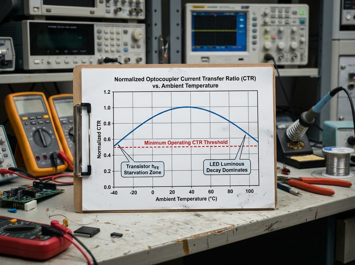
Emitter Degradation Mechanics (Arrhenius Aging)
Over continuous operating hours, non-radiative defect centers multiply within the LED crystal lattice[5]. Thermal stress accelerates this degradation in accordance with the Arrhenius relation:
Whereis the activation energy of defect formation (to, depending on wafer doping and epitaxial growth quality),is Boltzmann's constant, andis the junction temperature.
These defects capture injected carriers without releasing photons, progressively reducing optical radiant flux for a fixed drive current.
Opposing Thermal Dynamics
Ambient temperature variations impact the emitter and detector in opposite directions:
The Infrared Emitter (GaAs/AlGaAs): Demonstrates a negative temperature coefficient. As temperature rises, non-radiative thermal lattice vibrations increase, diminishing radiative quantum efficiency. Emitter photon flux drops at an approximate rate ofto.
The Silicon Phototransistor: Demonstrates a positive temperature coefficient. Thermal carrier excitation extends minority carrier lifetime in the silicon base region, causing common-emitter gain () to increase with rising temperature.
This interaction produces an inverted-U temperature profile. At sub-zero temperatures (e.g.,), the phototransistor'scollapses, suppressing overall CTR despite high photon output from the LED. At elevated temperatures (e.g.,), the phototransistor's gain plateau cannot compensate for the sharp decline in LED optical emission, causing CTR to roll off.
Hardware designers must evaluate both extreme hot and extreme cold operating bounds rather than assuming the hottest condition is uniquely worst-case.
3. The Worst-Case CTR Budget Framework (The Multiplicative Derating Model)
To prevent operational dropout, hardware engineers must calculate the minimum expected CTR at the absolute end of the product's design life.
The Engineering Derating Model
: Guaranteed datasheet lower bound for specified bin.
: Normalized derating at actual low drive current.
: Worst-case boundary factor across operating temperature.
: Mission-profile aging factor ().
: End-of-Life worst-case linear transfer ratio.
Parameter Extraction Protocol
| Variable | Description | Extraction Method | Typical Value Range () |
|---|---|---|---|
| Baseline CTR lower limit | Extracted directly from the datasheet electrical specifications table for the specified part suffix. | 100% to 200% (for Rank B/C types) | |
| Low-current normalization factor | Read from the Normalized CTR vs. Forward Current characteristic curve (). | 0.30 to 0.65 at | |
| Thermal envelope factor | The lowest value of the Normalized CTR vs. Ambient Temperature curve across the design envelope (to). | 0.70 to 0.85 acrossto | |
| Service life derating factor | Determined using vendor Arrhenius lifetime projection curves based on actual,, and service years (). | 0.75 to 0.85 (assuming 10–20 yr service) |
Linear CTR vs. Saturated CTR ()
Datasheets generally documentunder linear active conditions (typically). In digital interfacing circuits, however, the phototransistor must pull down a node into saturation ().
Under saturated conditions, the phototransistor's collector-base junction becomes forward-biased, sweeping stored charge into the base and drastically reducing effective collector current sink capability. As documented in Vishay Application Note 83706[1], the saturated Current Transfer Ratio () can be less than half of the linear active CTR under identical forward current conditions.
To guarantee saturation, designers must either extract parameters directly from the vendor's saturated characteristic curves () or apply an explicit saturation overdrive ratio:
4. Practical Design Walkthrough: Sizing a Low-Power Isolated Input Stage
Circuit Scenario
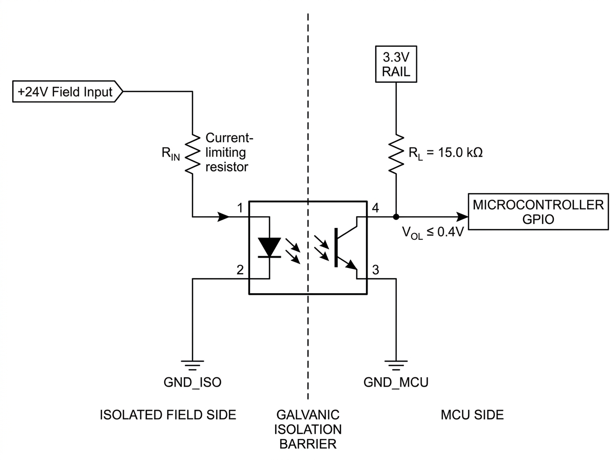
An industrial field input stage interfaces afield signal to amicrocontroller GPIO input (, required margin:). To minimize field power dissipation, the input dropping network drives an optocoupler LED with a minimum current of.
Operating Envelope:
Target Operating Lifetime: 10 years continuous operation ()
Component Selected: Industrial phototransistor optocoupler, guaranteed Rank B binning (at)
Derivation Steps
Step 1: Extract the Low-Current Multiplier ()
Consulting the manufacturer's Normalized CTR vs. Forward Current curve (normalized to):
Step 2: Extract the Operating Temperature Multiplier ()
Evaluating the Normalized CTR vs. Ambient Temperature curve acrossto:
At, low-temperature transistor gain drop yields.
At, LED radiant flux reduction yields.
Selecting the worst-case boundary:
Step 3: Extract the Multi-Year Aging Multiplier ()
From vendor lifetime projection charts (e.g., Toshiba AKX00788[4] or Renesas Lifetime curves[2]) atand, the 10-year optical emission wearout is projected at $20\%$:
Step 4: Calculate the Composite Worst-Case CTR ()
Step 5: Calculate Available Worst-Case Collector Sink Current ()
Step 6: Apply the Saturation Overdrive Factor ()
To enforce deep saturation () rather than operating on the verge of the linear active region, budget an overdrive factor:
Step 7: Size the Collector Pull-Up Resistor ()
To ensure the phototransistor pulls the MCU pin below:
Selecting the next higher standard E96 resistor value ensures the collector current remains below the maximum saturated capability:
Design Comparison: Nominal vs. Worst-Case
| Parameter | Nominal Condition (, Initial) | Worst-Case Condition (, 10-yr EOL) | Margin Impact |
|---|---|---|---|
| Forward Drive Current () | Primary input baseline | ||
| Effective CTR | $35.2\%$ | $-36\%$ relative loss | |
| Max Linear Sink Current () | Current sink capacity reduced | ||
| Target Saturated Sink Current | (Assumed) | Overdrive safety factor applied | |
| Max Permissible Pull-Up () | Usingwould cause EOL saturation failure | ||
| Calculatedat GPIO | (Using) | Logic zero integrity maintained |
5. The Hidden Dynamic Penalty: Bandwidth, Propagation Delay, and Saturation
Sizing large collector pull-up resistors () resolves DC saturation challenges at low drive currents, but introduces a severe dynamic penalty that can compromise digital signal integrity.
The Miller Effect at Low Collector Currents
A phototransistor possesses an internal collector-base capacitance (, typicallyto). The effective input capacitance of the stage is amplified by the circuit's voltage gain through the Miller effect:
When the phototransistor turns off, stored charge in the base must recombine, and the output node capacitance (including, trace capacitance, and MCU pin capacitance) must be recharged entirely through the collector pull-up resistor ().
Asscales fromtoto accommodate sub-milliamp forward currents, the turn-off delay () stretches from roughlyup to. This limits communication throughput to underand causes severe duty-cycle distortion.
Furthermore, slow output voltage slew rates () can cause input chatter or supply rail cross-conduction on non-Schmitt inputs. Low LED drive also degrades effective common-mode transient immunity (CMTI), as high-voltage transients () across barrier parasitic capacitance can more easily overwhelm the microamp-level signal current.
Feedback Loop Instability: The TL431 Sinking Trap
In isolated switched-mode power supplies (SMPS), the optocoupler forms the primary-to-secondary feedback path, typically driven by a TL431 adjustable shunt regulator. Hardware engineers attempting to lower no-load standby power often scale down optocoupler LED current below.
This introduces a catastrophic reliability hazard:
The TL431 internal reference architecture mandates a minimum cathode regulation current of[7] across its full operating temperature range to maintain internal bandgap stability.
If an engineer starves the optocoupler drive belowwithout placing a bypass bleed resistor in parallel with the optocoupler's LED, the TL431 loses loop regulation.
This loss of regulation manifests as high-amplitude low-frequency output voltage ripple, erratic burst-mode switching, and audible transformer hissing.
Troubleshooting SMPS Optocouplers: CTR Degradation, Failure Modes; Active Testing
6. Industry Pitfalls and Heuristic Gaps: Debunking Flat Derating Rules
| Common Industry Heuristic | Physical Semiconductor Reality | Hardware Failure Mechanism |
|---|---|---|
| "Apply a flat 50% derating rule to typical CTR for everything." | Emitter aging depends on junction temperature, forward current density, and chemical dopants. Flat derating ignores cold-temperature transistor drop-offs and space-charge recombination collapse. | Sizing pull-up resistors based on a flat 50% nominal value under-budgets low-current roll-off, causing high-temperature or end-of-life logic read errors. |
| "If an optocoupler has 100% CTR at, it gives 100% at." | CTR is non-linear. At,typically falls betweenand, reducing the baseline room-temperature CTR to just 30%–50%. | Collector sink current fails to reach design targets, pulling down the output node only partially and hovering between valid logic states. |
| "Sizing the collector pull-up using linear $CTR$ () is fine for GPIOs." | Saturation suppresses transistor gain. Drivingtoreduces effective current transfer by an additional 30% to 60% relative to active mode. | Output transistor fails to achieve a valid logic-low (floats above), causing missing pulse edges or stuck-high inputs. |
| "Testing pins with a digital multimeter (DMM) diode check proves the optocoupler is good." | A DMM diode check verifies basic PN junction continuity (drop on the LED) and un-shorted collector-emitter pins. It cannot evaluate luminous efficiency or CTR degradation. | Degraded parts exhibiting a 70% CTR loss test "pass" on a basic multimeter, masking impending field dropouts. |
7. Laboratory Validation Protocol: Four-Corner Bench Testing and Synthetic Aging
To validate worst-case optocoupler margins without waiting years for wearout to manifest, development teams must execute an accelerated bench verification protocol on physical prototype hardware.
Step 1: Synthetic Aging Emulation: Reduce bench drive to.
Step 2: Four-Corner Environmental Stress: Sweep thermal chamber across full envelope (to).
Step 3: Direct Saturation Headroom Verification: Measureunder loaded output: Must remain.
Step 4: Dynamic Slew-Rate and Timing Check: Verify,, andagainst receiver input specs.
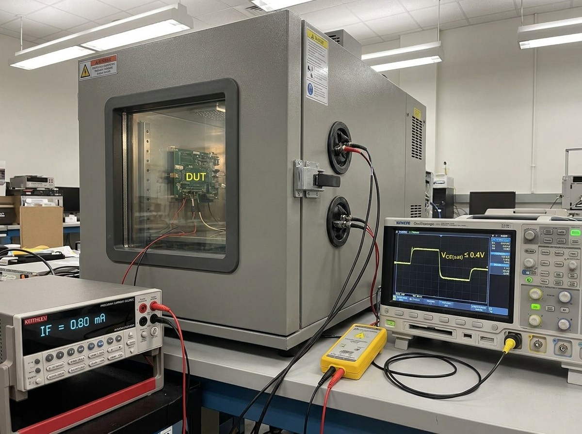
Step 1: Synthetic Aging Emulation (Current Starvation)
Emulate 10-to-20-year emitter optical decay directly on the test bench by artificially starving the input drive current. Calculate the test drive current using the aging factor:
Example: For an operating drive ofand a budgeted 10-year aging factor, adjust the bench programmable current source or input drive resistor to deliver exactly.
Step 2: Four-Corner Environmental Thermal Sweep
Place the board in an environmental thermal chamber while maintaining starved forward drive (). Execute test sweeps across four operational corners:
Corner 1:,(Tests phototransistor carrier starvation and minimum gain)
Corner 2:,(Tests pull-up load current peak at cold temperature)
Corner 3:,(Tests logic-low threshold headroom with heated LED decay)
Corner 4:,(Tests maximum thermal dissipation and leakage current,)
Step 3: Direct Saturation Headroom Verification
Probe the collector-emitter voltage () directly at the component pins while operating under worst-case starved conditions:
Ensureacross all four corners.
Verify a minimum noise margin between measuredand the receiving microcontroller's guaranteedinput threshold.
Step 4: Dynamic Transition & Slew-Rate Verification
Using active, low-capacitance oscilloscope probes (load), measure the rise time (), fall time (), and total propagation delay:
Confirm the output signal slew rate exceeds the minimum input edge rate specified by the receiving microcontroller to prevent internal clock oscillator instability or bus chatter.
Ensure maximum duty-cycle distortion remains within serial bus timing budgets (e.g., UART bit sampling windows).
Electrical Safety Warning for Isolated Probing
When performing bench measurements on optocouplers bridging isolated power domains (e.g., primary off-line mains to secondary low-voltage DC):
Never connect an earth-grounded oscilloscope ground clip to the floating primary high-voltage bus. Doing so creates a low-impedance short circuit to earth ground through the mains supply, destroying test instrumentation and presenting an electrical shock hazard.
Always employ high-voltage differential probes or an isolated-channel oscilloscope when probing signals spanning the galvanic barrier.
8. Component Selection Boundaries: When to Pivot Beyond Phototransistors
When system requirements push input forward current belowor require transmission speeds above a few kilobits per second, standard phototransistor optocouplers become impractical. The table below outlines architectural boundaries across primary isolation technologies.
| Isolation Technology | Typical Drive Requirements | CTR / Gain Stability Over 10+ Years | Saturation Output () | Max Bandwidth / Data Rate | Standby Power Overhead | Relative BOM Cost | Recommended Industrial Use Cases |
|---|---|---|---|---|---|---|---|
| Standard Phototransistor | Moderate to Poor (Subject to compound aging and thermal drift) | Low () | Very Low (at low power) | Zero secondary quiescent current | Baseline () | Static DC status inputs, low-speed interlocks, slow feedback loops. | |
| Darlington-Output Optocoupler | Poor (High initial gain, but severe thermal leakage drift) | High () | Extremely Low (due to base charge trapping) | Zero secondary quiescent current | Low-to-Medium () | Low-current relay or solenoid driving where output saturation voltage is non-critical. | |
| Active-Detector Optocoupler (Digital Output) | High (Integrated amplifier and threshold comparator circuit) | Excellent (rail-to-rail) | Medium-to-High () | Requires secondarysupply () | Medium () | Isolated industrial SPI, UART, and PWM fieldbus links requiring optical immunity. | |
| Digital Isolators[6] (Capacitive / Magnetic) | None (Logic input buffer:) | Exceptional (Zero optical decay; flat acrossto) | Excellent (CMOS push-pull output) | Ultra-High () | Requires primary and secondarysupplies | Medium-to-High () | High-speed multi-channel data acquisition, high-temperature industrial environments. |
Summary Decision Boundaries
Maintain Standard Phototransistors: When forward current budget satisfies, operating temperature does not exceed, switching speeds remain below, and minimizing bill-of-materials cost is paramount.
Avoid Darlington Outputs for Microcontroller Inputs: Darlington optocouplers provide high transfer ratios at sub-milliamp drive, but their internal saturation voltage () violates standardorCMOS logic-low thresholds (), requiring external level-shifting buffers.
Pivot to Active Optocouplers or Digital Isolators: When available input current falls below, data transmission rates exceed, industrial environments demand high common-mode transient immunity (CMTI), operating temperatures reachor higher, or long operational service lives () require elimination of optical drift.
9. Frequently Asked Questions (FAQ)
Can an unbinned PC817 be safely used in a low-power industrial input circuit?
No. Standard unbinned commodity PC817 optocouplers span an expansive 50% to 600% CTR window. Sizing a circuit to guarantee saturation using the 50% lower limit forces high LED drive current, defeating low-power goals.
Conversely, if a 600% CTR component from that same unbinned lot is installed in production, its collector will drive into extreme saturation, producing long turn-off storage times () that distort switching edges. Designers should always specify sorted bins (e.g., PC817B: 130%–260%, or PC817C: 200%–400%).
How does optocoupler CTR differ fundamentally from a standard BJT's?
Bipolar junction transistor current gain () is a purely electronic ratio between collector current and base current ().
In contrast, optocoupler Current Transfer Ratio () is an end-to-end electro-optical transfer function that encompasses:
Electrical-to-optical conversion efficiency within the infrared LED ().
Physical geometry and optical transmission efficiency of the internal insulating barrier.
Optical-to-electrical conversion efficiency of the detector's collector-base photodiode.
Electronic current gain () of the output phototransistor structure.
Why do optocouplers with an external base pin exhibit higher noise at low currents, and should a base resistor be used?
The external base terminal (Pin 6 on 6-pin DIP optocouplers) connects directly to the phototransistor's sensitive collector-base junction. In low-current designs operating with high collector load resistances, this high-impedance pin acts as an antenna that couples high-voltage transients () across the isolation barrier.
Connecting a high-value resistor () between base and emitter drains away capacitive displacement currents and accelerates stored base-charge turn-off. However, it also shunts useful photocurrent away from the base, significantly reducing overall CTR. For low-current digital inputs, specify 4-pin optocouplers that omit the external base pin entirely.
Does operating an LED at low forward current eliminate the need for temperature derating?
No. Operating at low forward current virtually eliminates internal junction self-heating (), which prevents thermally accelerated Arrhenius wearout.
However, it does not isolate the device from ambient environmental shifts. Extreme cold (e.g.,) reduces phototransistor, while elevated ambient heat (e.g.,) degrades LED photon generation efficiency. Temperature derating across the target environmental range remains mandatory.
10. Pre-Tapeout Low-Power Optocoupler Checklist
Review these eight verification gates before releasing schematics and bills of materials to production:
[ ] BOM Rank Specificity: The bill of materials specifies a narrow CTR bin/rank suffix (e.g.,
PC817B,TLP185(GB), orCNY17F-2) rather than a generic base part number.[ ] Derating Derivation Documented: Sizing calculations explicitly account for,, and, with all derating multipliers traceable to manufacturer datasheet curves.
[ ] Saturation Overdrive Enforced: Collector pull-up resistor sizing incorporates a minimum saturation overdrive factor () to guarantee deep saturation ().
[ ] Logic Threshold Margin Verified: Worst-caseunder full load and starved drive leaves at leastof noise margin below the receiving logic gate'sspecification.
[ ] Timing & Propagation Delay Validated: The RC charging time constant formed byand node capacitance does not violate serial bus bit-timing or microcontroller edge-rate limits.
[ ] Shunt Regulator Bias Verified: If interfacing to a TL431 in a feedback loop, verify that the regulator's minimum cathode current () is satisfied across all line and load conditions.
[ ] Synthetic Aging Bench-Tested: Prototype hardware has passed functional validation under starved input drive () inside an environmental chamber across minimum and maximum operating temperatures.
[ ] High-Voltage Probing Protocol Enforced: Bench qualification procedures require isolated differential probes for measurements bridging isolated grounds, preventing instrument ground loops.
Sources and references used for this guide
How to Use Optocoupler Normalized Curves (Application Note 83706)
Source type: official company documentation
Used for: Mathematical framework for normalizing CTR across forward currents and operating temperatures, saturation derating calculations, and pull-up resistor sizing.
Caution: Curves depict typical relative behavior; absolute minimum design baselines must be pegged to guaranteed datasheet rank limits.Lifetime of Optocoupler/Photocoupler (Application Note)
Source type: official company documentation
Used for: Solid-state physical models of LED luminous degradation, Arrhenius lifetime acceleration formulas, and forward-current aging dependencies.
Caution: Specific lifetime projection curves apply to Renesas PS/RV1S series emitter dopants and must be adjusted for other manufacturer processes.Lifetime of Optocouplers (Application Note ANO006a)
Source type: official company documentation
Used for: Empirical evidence demonstrating that reduced LED forward current and reduced ambient temperature significantly decelerate long-term CTR degradation.
Caution: Focuses on emitter wear-out; does not eliminate the requirement to calculate initial low-current CTR non-linear collapse.Basic Characteristics and Application Circuit Design of Photocouplers (Application Note AKX00788)
Source type: official company documentation
Used for: Multi-year degradation curves for commercial optocouplers (TLP series), practical 10-year aging allowances (20% to 30%), and switching circuit design rules.
Caution: Aging allowances assume moderate operating temperatures; high-temperature industrial environments require higher derating margins.Optocouplers White Paper: LED Reliability Stress Data
Source type: official company documentation
Used for: Accelerated stress testing data, LED emitter crystal defect mechanics, and formal definition of Current Transfer Ratio.
Caution: Data reflects Broadcom proprietary optocoupler construction and hermetic/optocoupler packaging standards.Improve Your System Performance by Replacing Optocouplers (SLLA526)
Source type: official company documentation
Used for: Comparative reliability analysis between traditional optocoupler aging drift and solid-state digital isolation alternatives.
Caution: Vendor source advocating for digital isolators; must be balanced with optocoupler cost and passive input benefits.Make sure your optocoupler is properly biased (SSZTCW5)
Source type: official company documentation
Used for: Circuit biasing requirements to guarantee saturated collector operation and avoid erroneous logic switching.
Caution: Application brief focused on specific power conversion feedback topologies; general input circuits must adapt the formulas.General Description - Optocouplers (Document 80059)
Source type: official company documentation
Used for: Baseline optocoupler construction standards, isolation voltage ratings (5300 VRMS), and failure mechanism definitions.
Caution: Broad foundational document; specific electrical parameter limits must be confirmed in individual part datasheets.
 UTMEL
UTMEL
We are the professional distributor of electronic components, providing a large variety of products to save you a lot of time, effort, and cost with our efficient self-customized service. careful order preparation fast delivery service
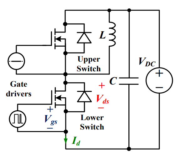 Discovering New and Advanced Methodology for Determining the Dynamic Characterization of Wide Bandgap DevicesSaumitra Jagdale15 March 20242837
For a long era, silicon has stood out as the primary material for fabricating electronic devices due to its affordability, moderate efficiency, and performance capabilities. Despite its widespread use, silicon faces several limitations that render it unsuitable for applications involving high power and elevated temperatures. As technological advancements continue and the industry demands enhanced efficiency from devices, these limitations become increasingly vivid. In the quest for electronic devices that are more potent, efficient, and compact, wide bandgap materials are emerging as a dominant player. Their superiority over silicon in crucial aspects such as efficiency, higher junction temperatures, power density, thinner drift regions, and faster switching speeds positions them as the preferred materials for the future of power electronics.
Read More Applications of FPGAs in Artificial Intelligence: A Comprehensive GuideUTMEL29 August 20255483
This comprehensive guide explores FPGAs as powerful AI accelerators that offer distinct advantages over traditional GPUs and CPUs. FPGAs provide reconfigurable hardware that can be customized for specific AI workloads, delivering superior energy efficiency, ultra-low latency, and deterministic performance—particularly valuable for edge AI applications. While GPUs excel at parallel processing for training, FPGAs shine in inference tasks through their adaptability and power optimization. The document covers practical implementation challenges, including development complexity and resource constraints, while highlighting solutions like High-Level Synthesis tools and vendor-specific AI development suites from Intel and AMD/Xilinx. Real-world applications span telecommunications, healthcare, autonomous vehicles, and financial services, demonstrating FPGAs' versatility in mission-critical systems requiring real-time processing and minimal power consumption.
Read More The 2026 Engineer’s Guide: Choosing the Right MCU for Your Next IoT & New Energy ProjectUTMEL30 April 20261638
A comprehensive comparison of 2026's leading MCUs from ST, NXP, and Microchip across power efficiency, processing performance, connectivity, and ecosystems to help engineers select the optimal chip for next-gen IoT and new energy projects.
Read More AI Server Components: Engineering Next-Gen Data Center Hardware for 100kW RacksUTMEL15 May 2026899
The transition from traditional enterprise IT to AI-driven workloads has rendered legacy data center hardware obsolete, forcing infrastructure planners to re-engineer server components for extreme thermal environments.
Read More The Practical Engineer’s Guide to the NE555N Timer: Pinout, Setup, and TroubleshootingUTMEL29 May 2026681
This comprehensive guide explores the NE555N timer, detailing its 8-pin layout, internal architecture, and key datasheet specifications. It compares the bipolar IC to CMOS variants and details setup configurations for astable, monostable, and bistable modes. Additionally, the guide offers practical troubleshooting advice to prevent common breadboard failures, such as floating reset pins and electrical noise issues.
Read More
Subscribe to Utmel !
![ATSHA204A-RBHCZ-B]() ATSHA204A-RBHCZ-B
ATSHA204A-RBHCZ-BMicrochip Technology
![ACPL-K342-560E]() ACPL-K342-560E
ACPL-K342-560EBroadcom Limited
![1EDC40I12AHXUMA1]() 1EDC40I12AHXUMA1
1EDC40I12AHXUMA1Infineon Technologies
![HCS362T-I/SN]() HCS362T-I/SN
HCS362T-I/SNMicrochip Technology
![AT88SC0104CA-TH-T]() AT88SC0104CA-TH-T
AT88SC0104CA-TH-TMicrochip Technology
![ADATE304BBCZ]() ADATE304BBCZ
ADATE304BBCZAnalog Devices Inc.
![DLP3310FQM]() DLP3310FQM
DLP3310FQMTexas Instruments
![FOD3182V]() FOD3182V
FOD3182VON Semiconductor
![FM31256-G]() FM31256-G
FM31256-GCypress Semiconductor Corp
![HCPL-3180-000E]() HCPL-3180-000E
HCPL-3180-000EBroadcom Limited


